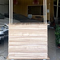
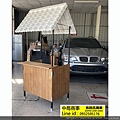
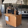
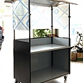
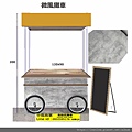
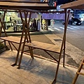
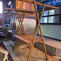
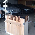
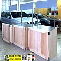
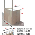
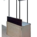
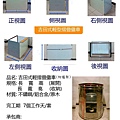
1.快拆秒收摺疊
2.輕量 / 防火 / 防鏽
3.白鐵 / 鋁合金 材質
4.移動範圍最遠
5.攜帶量最大
6.淨量6公斤
7.荷重60公斤
2.輕量 / 防火 / 防鏽
3.白鐵 / 鋁合金 材質
4.移動範圍最遠
5.攜帶量最大
6.淨量6公斤
7.荷重60公斤
上一頁下一頁

Sogo用折疊+手推攤車藍色

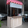
小丸子攤車

市集兩用4尺快閃餐車2

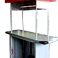
市集用4尺快閃餐車

快閃攤車餅乾拷貝

台南快閃甜點攤車

413262169_1570009733796285_3677309033283009242_n

仁慈攤車4

仁慈攤車3

仁慈攤車2

仁慈攤車5
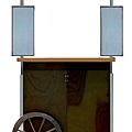
手推折疊攤車231110c
手推折疊攤車231110b
IMG_5311手推折疊攤車231110d
手推折疊攤車231110a
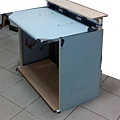
農集商場專用折疊攤車2

快閃爐具用早餐車
LINE_P20221029_15351213
防疫早餐車2
微風攤車3
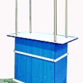
Sogo用折疊+手推攤車藍色
Sogo用折疊+手推攤車1
Sogo用折疊+手推攤車
折疊式手推攤車-胖卡造型
快閃攤車餅乾
gogoro電動車攜帶用折疊攤車
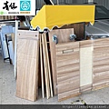
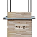
木造折疊攤車2
木造折疊攤車1

關西廟會攤車
咖啡攤車4門轎車攜帶
LINE_P20190522_080027804

BBQ-VENDER-BY-FORDING
原木外牆攤車2
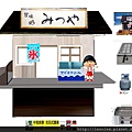
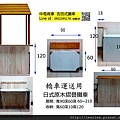
日式摺疊攤車雲林
透明海灣櫃攤車

胖卡摺疊攤車2

vw-T1呂合金掛板
zakka攤車
zakka攤車2
木造摺疊攤車群

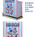
kitty三麗鷗

國民攤車-雞蛋糕
輕食銷售用攤車

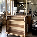
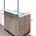
四尺摺疊攤車
休旅車攜帶四尺摺疊攤車1

轎車攜帶三尺摺疊攤車
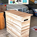
原木摺疊攤車
四尺摺疊原木攤車1
轎車攜帶三尺摺疊攤車

休旅車攜帶四尺摺疊攤車1
1480047295431
1480086050088

LINE掃描
pokemon-vender-

pokemon-vender-2--

五門車輛用碳燒烤摺疊攤車

福岡屋台 - folding vendor

博多屋台 - folding vendor
白鐵摺疊攤車1

妖怪夜市攤車
櫻桃小丸子攤車

吉野家碳烤攤車
開孔用攤車附爐架
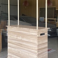
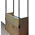
原木屋頂折疊攤車
古早味摺疊式原木攤車
立體原木摺疊攤車全視圖

摺疊屋頂攤車
關東煮原木摺疊攤車
輕量無輪摺疊攤車

灣流型攤車-付透明櫥窗

國民雞蛋糕

轎車運送專用/原木外牆
PIZZA店直營店專用

卡通地毯的裝飾應用
機車踏板運送專用攤車

摺疊攤車快速收納-輕便好攜帶-
摺疊攤車收納背圖
摺疊攤車快速收納-輕便好攜帶-
上一頁下一頁
分享:


相片最新留言
-
 王妃 說:請問一下老板,日式zakka 木...
 -

-
amy 說:請問 長,寬,高 是否能加...
-
-
 Iverson Tsai 說:我想尋問,這款的尺寸與報價...
此相簿內的相片出現在:
- folding vendor 免費脆皮雞蛋糕教學做法烘焙摺疊餐車--胖卡攤車設計製作轎車運送腳踏車拖曳攜帶用 一例一休 創業營業用卡通脆皮雞蛋糕配方- 吉田製作所 -第二專長培訓
- 免費脆皮雞蛋糕教學烘焙餐車--攤車設計製作轎車運送腳踏車拖曳用- 週休二日~創業營業用卡通脆皮雞蛋糕配方 - 吉田製作所 -第二專長培訓
- 免費脆皮雞蛋糕做法教學烘焙餐車--胖卡攤車設計製作轎車運送腳踏車拖曳藏壽司行動攤車攜帶用 一例一休~創業營業用卡通脆皮雞蛋糕配方 - 吉田製作所 -第二專長培訓
- 行動早餐車新品登場 - 戶外用手作天津煎餅果子/現烤義大利披薩攤車/現烤盒酥脆皮三明治 - 美式厚片義式薄片芝心披薩餅皮披薩醬義大利醬製作教學
- 廣告用快閃店攤車設計百貨公司與商展專用 吉田式摺疊攤車與定著式攤車 - 店門口戶外用飲料冰品專用櫃檯
相簿列表資訊
- 最新上傳:
- 2024/11/27
- 全站分類:
- 美食記錄
- 本日人氣:
- 0
- 累積人氣:
- 7415

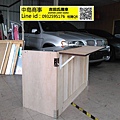
請問灣流型攤車價錢多少
To Sara:
請問是賣雞蛋糕?
款式分為
摺疊與手推與拖曳
規格可分
3尺4尺5尺
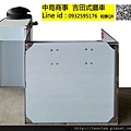
請line 我們
ID: 0932595176
常見的半導體材料有矽、鍺、砷化鎵等
/
晶片測試
晶片處理高度有序化的本質增加了對不同處理步驟之間度量方法的需求。晶片測試度量裝置被用於檢驗晶片仍然完好且沒有被前面的處理步驟損壞。如果If the number of dies—the 積體電路s that will eventually become chips—當一塊晶片測量失敗次數超過一個預先設定的閾值時,晶片將被廢棄而非繼續後續的處理製程。
/
晶片測試
晶片處理高度有序化的本質增加了對不同處理步驟之間度量方法的需求。晶片測試度量裝置被用於檢驗晶片仍然完好且沒有被前面的處理步驟損壞。如果If the number of dies—the 積體電路s that will eventually become chips—當一塊晶片測量失敗次數超過一個預先設定的閾值時,晶片將被廢棄而非繼續後續的處理製程。
/
步驟列表
晶片處理
濕洗
平版照相術
光刻Litho
離子移植IMP
蝕刻(干法蝕刻、濕法蝕刻、電漿蝕刻)
熱處理
快速熱退火Annel
熔爐退火
熱氧化
化學氣相沉積 (CVD)
物理氣相沉積 (PVD)
分子束磊晶 (MBE)
電化學沉積 (ECD),見電鍍
化學機械平坦化 (CMP)
IC Assembly and Testing 封裝測試
Wafer Testing 晶片測試
Visual Inspection外觀檢測
Wafer Probing電性測試
FrontEnd 封裝前段
Wafer BackGrinding 晶背研磨
Wafer Mount晶圓附膜
Wafer Sawing晶圓切割
Die attachment上片覆晶
Wire bonding焊線
BackEnd 封裝後段
Molding模壓
Post Mold Cure後固化
De-Junk 去節
Plating 電鍍
Marking 列印
Trimform 成形
Lead Scan 檢腳
Final Test 終測
Electrical Test電性測試
Visual Inspection光學測試
Baking 烘烤
/
有害材料標誌
許多有毒材料在製造過程中被使用。這些包括:
有毒元素摻雜物比如砷、硼、銻和磷
有毒化合物比如砷化三氫、磷化氫和矽烷
易反應液體、例如過氧化氫、發煙硝酸、硫酸以及氫氟酸
工人直接暴露在這些有毒物質下是致命的。通常IC製造業高度自動化能幫助降低暴露於這一類物品的風險。
/
Device yield
Device yield or die yield is the number of working chips or dies on a wafer, given in percentage since the number of chips on a wafer (Die per wafer, DPW) can vary depending on the chips' size and the wafer's diameter. Yield degradation is a reduction in yield, which historically was mainly caused by dust particles, however since the 1990s, yield degradation is mainly caused by process variation, the process itself and by the tools used in chip manufacturing, although dust still remains a problem in many older fabs. Dust particles have an increasing effect on yield as feature sizes are shrunk with newer processes. Automation and the use of mini environments inside of production equipment, FOUPs and SMIFs have enabled a reduction in defects caused by dust particles. Device yield must be kept high to reduce the selling price of the working chips since working chips have to pay for those chips that failed, and to reduce the cost of wafer processing. Yield can also be affected by the design and operation of the fab.
Tight control over contaminants and the production process are necessary to increase yield. Contaminants may be chemical contaminants or be dust particles. "Killer defects" are those caused by dust particles that cause complete failure of the device (such as a transistor). There are also harmless defects. A particle needs to be 1/5 the size of a feature to cause a killer defect. So if a feature is 100 nm across, a particle only needs to be 20 nm across to cause a killer defect. Electrostatic electricity can also affect yield adversely. Chemical contaminants or impurities include heavy metals such as Iron, Copper, Nickel, Zinc, Chromium, Gold, Mercury and Silver, alkali metals such as Sodium, Potassium and Lithium, and elements such as Aluminum, Magnesium, Calcium, Chlorine, Sulfur, Carbon, and Fluorine. It is important for those elements to not remain in contact with the silicon, as they could reduce yield. Chemical mixtures may be used to remove those elements from the silicon; different mixtures are effective against different elements.
Several models are used to estimate yield. Those are Murphy's model, Poisson's model, the binomial model, Moore's model and Seeds' model. There is no universal model; a model has to be chosen based on actual yield distribution (the location of defective chips) For example, Murphy's model assumes that yield loss occurs more at the edges of the wafer (non-working chips are concentrated on the edges of the wafer), Poisson's model assumes that defective dies are spread relatively evenly across the wafer, and Seeds's model assumes that defective dies are clustered together.[25]
Smaller dies cost less to produce (since more fit on a wafer, and wafers are processed and priced as a whole), and can help achieve higher yields since smaller dies have a lower chance of having a defect. However, smaller dies require smaller features to achieve the same functions of larger dies or surpass them, and smaller features require reduced process variation and increased purity (reduced contamination) to maintain high yields. Metrology tools are used to inspect the wafers during the production process and predict yield, so wafers predicted to have too many defects may be scrapped to save on processing costs.[26]